In 2029, the Large Hadron Collider’s high-luminosity upgrade (HL-LHC) will increase its integrated luminosity by a factor of 10 beyond its current design value, enabling the facility to collect increased amounts of data for experiments that observe rare physical processes.
Significant technological advancements are being developed to address these challenges, and to align and optimize their engineering efforts, the ATLAS and CMS experiments have formed an R&D collaboration (RD53) to design and develop a new hybrid pixel readout chip with improved functionality to serve both experiments’ detectors in the new HL-LHC era.
To accommodate this new technology, the ATLAS experiment is completely replacing its Inner Detector with a multi-layered all-silicon Inner Tracker (ITK), which will consist of pixel and strip detectors that are being designed to resolve more than 200 simultaneous particle collisions every 25 ns. In particular, the innermost layers of ATLAS’ pixel detectors will need to withstand the most challenging environment high-energy physics collider detectors have ever encountered, requiring enhanced technology that satisfies the following requirements:
- Radiation tolerant up to 1Grad total ionizing dose,
- 50 um by 50 um pixel pitch,
- Low noise (<100 e) and low power (<5 uW) per pixel pre-amplifiers,
- Process 3GHz/cm2 hit-rate,
- Buffer the data for up to 12.5us,
- Triggered data readout at 1MHz, requiring up to 5Gbps data links.
Berkeley Lab has been a core member of RD53 from the very beginning, playing a key role in multiple stages of the project. Since the founding of RD53 in 2013, the Engineering Division’s Integrated Circuit (IC) design team, along with scientists from the Physics Division’s ATLAS group, have collaborated with engineers and scientists from institutes around the world to design the new readout chip. Maurice Garcia-Sciveres – a senior staff scientist in Berkeley Lab’s Physics Division and a co-spokesperson for the ATLAS side of RD53 since its inception – notes that “forming the RD53 collaboration enabled us to develop a system-on-chip rivaling commercial microprocessors. This was needed to meet the requirements of the HL-LHC ATLAS and CMS experiments, but no single lab or experiment had the expert resources to do this on their own. Almost 100 person-years of IC design engineer time have gone into the RD53 chips, shared across personnel from 20 institutions, including LBNL.”
The Berkeley Lab team’s main contribution to RD53 is the differential front-end. This design concept was first tested in two early prototype chips – FE65-P1 and FE65-P2 – that were used to optimize the performance of the analog front-end, and they also served as an early test bed for the then-new 65nm CMOS (complementary metal-oxide semiconductor) technology. The FE65-P1 chip actually predated the formation of RD53 and provided the early technical foundation needed for the RD53 proposal to CERN. Dario Gnani, an IC Design Engineer in the Electronics, Software & Instrumentation Engineering Department of the Engineering Division, contributed to the initial prototype designs (analog islands design and FE65-P2) and then made most of the modifications required to meet the new specifications for RD53A. “The RD53 and satellite projects were a great opportunity to contribute to a major project and learn new skills also from our European colleagues, at CERN and Bonn in particular. I consider it a foundational experience in my career and a great personal experience.”
The first large-scale demonstrator chip (2cm by 1cm, with 76,800 pixels) was the RD53A chip, which included three different analog front-ends. Because power density was a major concern for the ITk Pixel detector, the ATLAS collaboration chose the differential front-end designed by LBNL for its very low noise at comparatively low power consumption. During the process of analyzing and finding design solutions, limitations were found in the extreme temperature and radiation tolerance conditions of the first full-scale RD53A prototype. Amanda Krieger, also an IC Design Engineer in Berkeley Lab’s Engineering Division, was responsible for further developing the analog front-end design and made significant improvements at this stage to address radiation hardness concerns. “The succession of design improvements – from RD53A through to the ITkPix series of large-scale ASICs – revealed the extensive effort of integrating many complex designs from multiple institutions into a functional ‘symphony.’” She added, “The 6 years that I have been part of the collaboration have been some of the most rewarding and enjoyable in my career, owing to both the impressive competencies of the engineers and physicists involved, and to the warm camaraderie of the collaboration.”
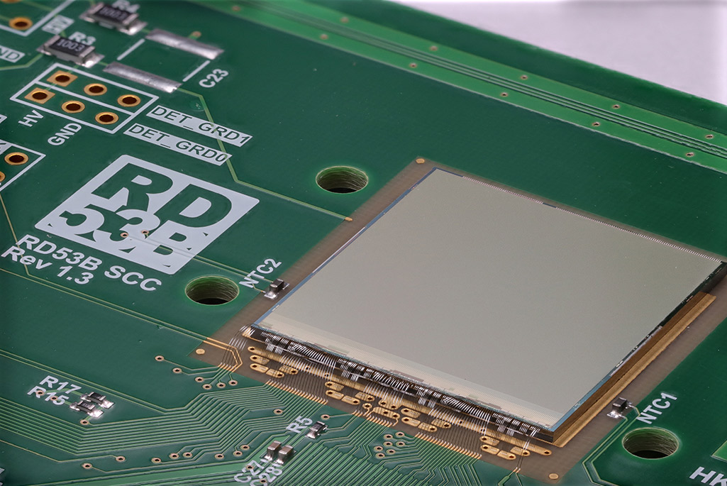 The pre-production chip for the ITk Pixel detector was called the ITkPixV1, a full-size (2cm by 2cm, 153,600 pixels) chip produced in March 2020 that included all of the necessary features for radiation tolerance. (Photo right: A bare ITkPixV1 readout chip mounted to single chip carrier card for testing purposes. Credit: Timon Heim, Berkeley Lab.) After several months of production and testing, the ITkPixV1 readout chip allowed the team to fully verify all detector concepts and requirements, and the ITkPixV1 was used to assemble a large number of detector modules to be deployed in systems tests. This stage also provided in-silicon feedback to the design of ITkPixV2, the final production chip for the ITK Pixel detector, marking a new era of pixel detectors at collider experiments.
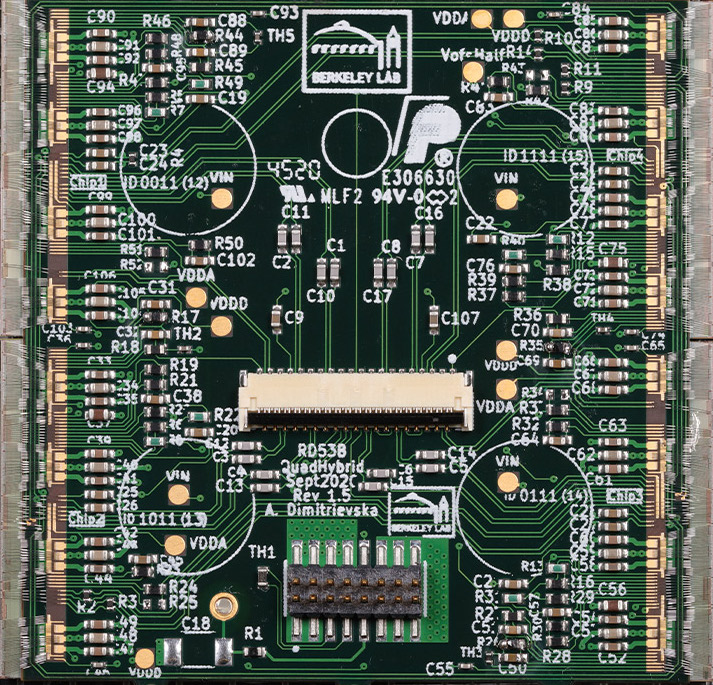 The ITk Pixel detector primarily uses quad modules, which combine 4 readout chips with 1 sensor that are equipped with a flex PCB to connect it to its electrical services. These modules are loaded onto carbon support structures to provide cooling and mechanical support. The LBNL Engineering team also specializes in these ultra-light carbon supports and will produce them for the innermost two layers of the ITk Pixel detector. (Photo right: A fully dressed ITkPixV1 Quad Module. 4 chips are connected to 1 sensor tile (4cm by 4cm) onto which a flex PCB is glued to connect to power and data services. Credit: Timon Heim, Berkeley Lab.) Now, after 2 years of design verification and production, the ITkPixV2 chip is now back at Berkeley Lab and being tested.
Timon Heim, a research scientist in Berkeley Lab’s Physics Division who oversees RD53 testing and participated in the chip design & development, explains that “ITkPixV2 is the culmination of 10 years of R&D and will set a new precedent for pixel detector technology. This would have not been possible without the excellent people within the RD53 collaboration and I hope future endeavors will be equally enjoyable and rewarding.”
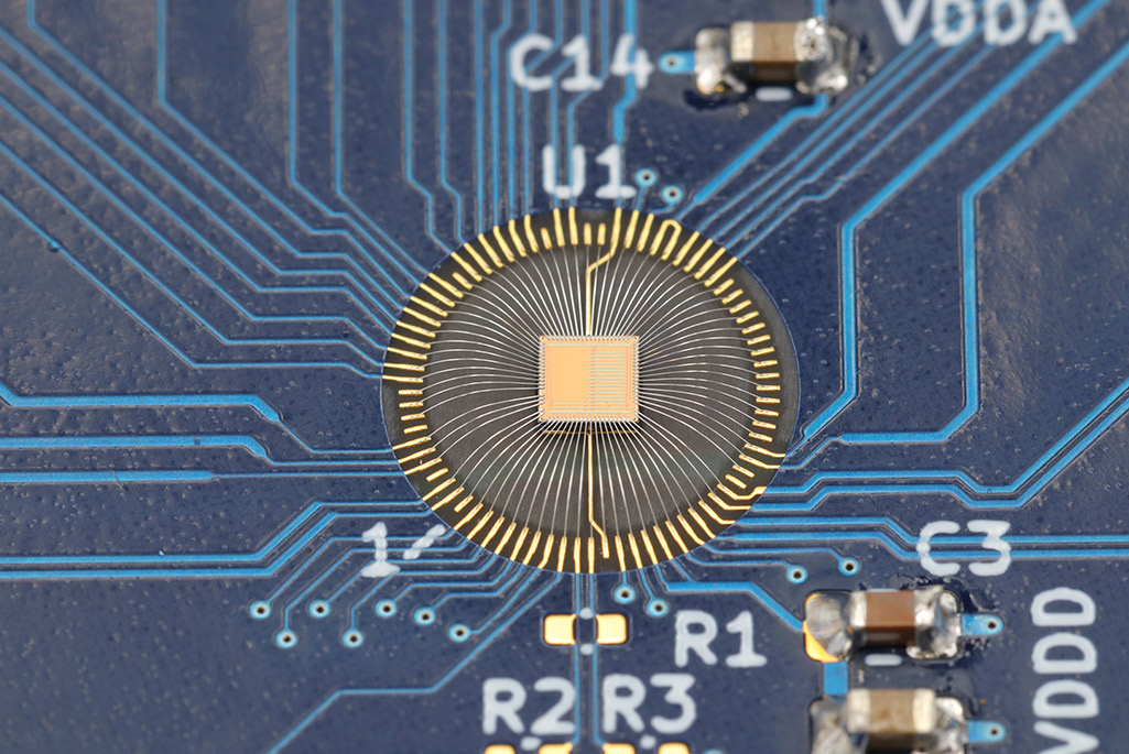
With the design of readout chips for the initial HL-LHC era coming to a close, the Berkeley Lab is already working on potential technology advancements for future generations of pixel detectors: 28nm CMOS. The first prototype ASICs now add timing information for an even more advanced analog front-end design, paving the way for future 4D trackers. (Photo below: Pebbles – a 28nm CMOS prototype ASIC to develop a pixel detector front-end that is low noise, low power, and has 100ps timing precision. Credit: Timon Heim, Berkeley Lab.)
Read More:
RD53 pixel chips for the ATLAS and CMS Phase-2 upgrades at HL-LHC – Slide presentation by Flavio Loddo (for the RD53 collaboration) on September 8, 2023, for PSD13: The 13th International Conference on Position Sensitive Detectors
First results from the ATLAS ITkPixV2 Readout Chip – Slide presentation by Maria Mironova (for the RD53 collaboration) on September 8, 2023, for PSD13: The 13th International Conference on Position Sensitive Detectors
Characterization of the BigRock 28 nm Fast Timing Analog Front End – Slide presentation by Amanda Krieger et al on October 3, 2023, for TWEPP 2023 Topical Workshop on Electronics for Particle Physics
RD53B Manual – CERN Publication Manual last updated by Maurice Garcia-Sciveres et al on September 27, 2021