In 2029, the Large Hadron Collider’s high-luminosity upgrade (HL-LHC) will increase its integrated luminosity by a factor of 10 beyond its current design value, enabling the facility to collect increased amounts of data for experiments that observe rare physical processes.
The upgrade will require new detectors and electronics that can handle high particle densities and high radiation levels, and significant technological advancements are being developed to address these challenges. To accommodate these advancements, the ATLAS experiment is completely replacing its Inner Detector with a multi-layered all-silicon Inner Tracker (ITk) that will extend its capabilities to precisely track charged particles.
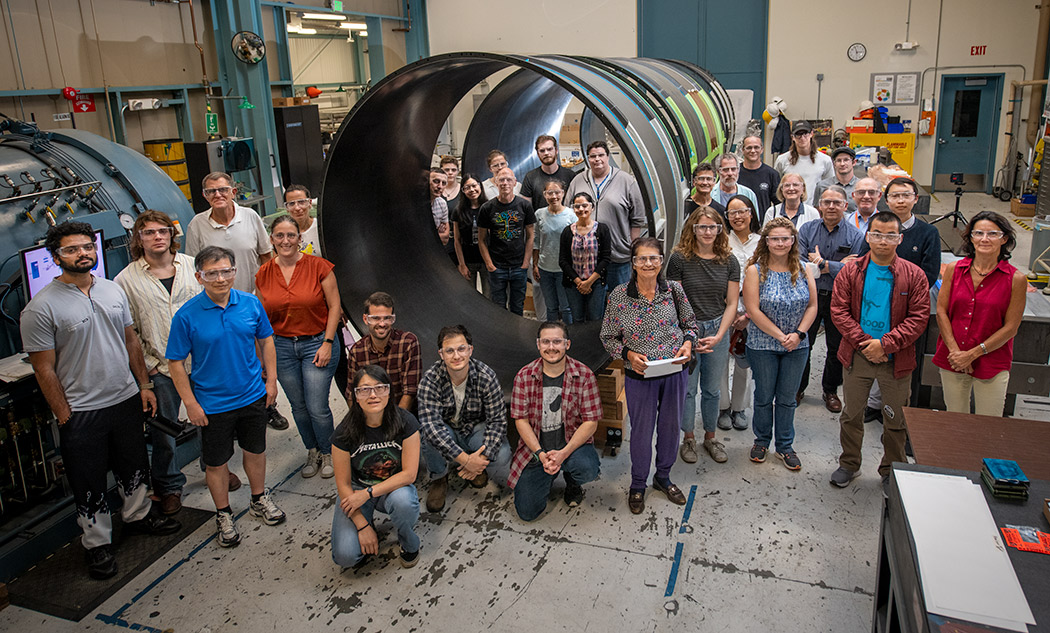 The ITk is a hierarchical structure in which highly specialized silicon sensors are enclosed in a series of nested cylindrical carbon fiber “barrel shells” that provide global support. These barrel shells are designed and fabricated at Berkeley Lab as part of a large collaboration between the Physics and Engineering Divisions. (Photo right: Berkeley Lab’s ATLAS research group poses next to the outer barrel shell. Photo credit: Thor Swift, November 2023.)
At ITk’s center, the innermost barrel shells enclose the finer-resolution ‘pixel sensors’ (also being developed at Berkeley Lab). The strip sensors are located in the next barrel shell layers around the pixel sensors. Each strip sensor is connected to an array of front-end electronics that can measure the signals of charged particles moving through the enormous ATLAS detector. The sensors process these measurements and send them to the ATLAS external data acquisition system.
The combination of a sensor and its associated front-end electronics is referred to as a “module,” and these are the basic electronic components of the ITk. A significant portion of ITk’s fabrication effort encompasses the assembly and testing of modules, and this work is being carried out at numerous research sites around the world, all part of the ATLAS Collaboration.
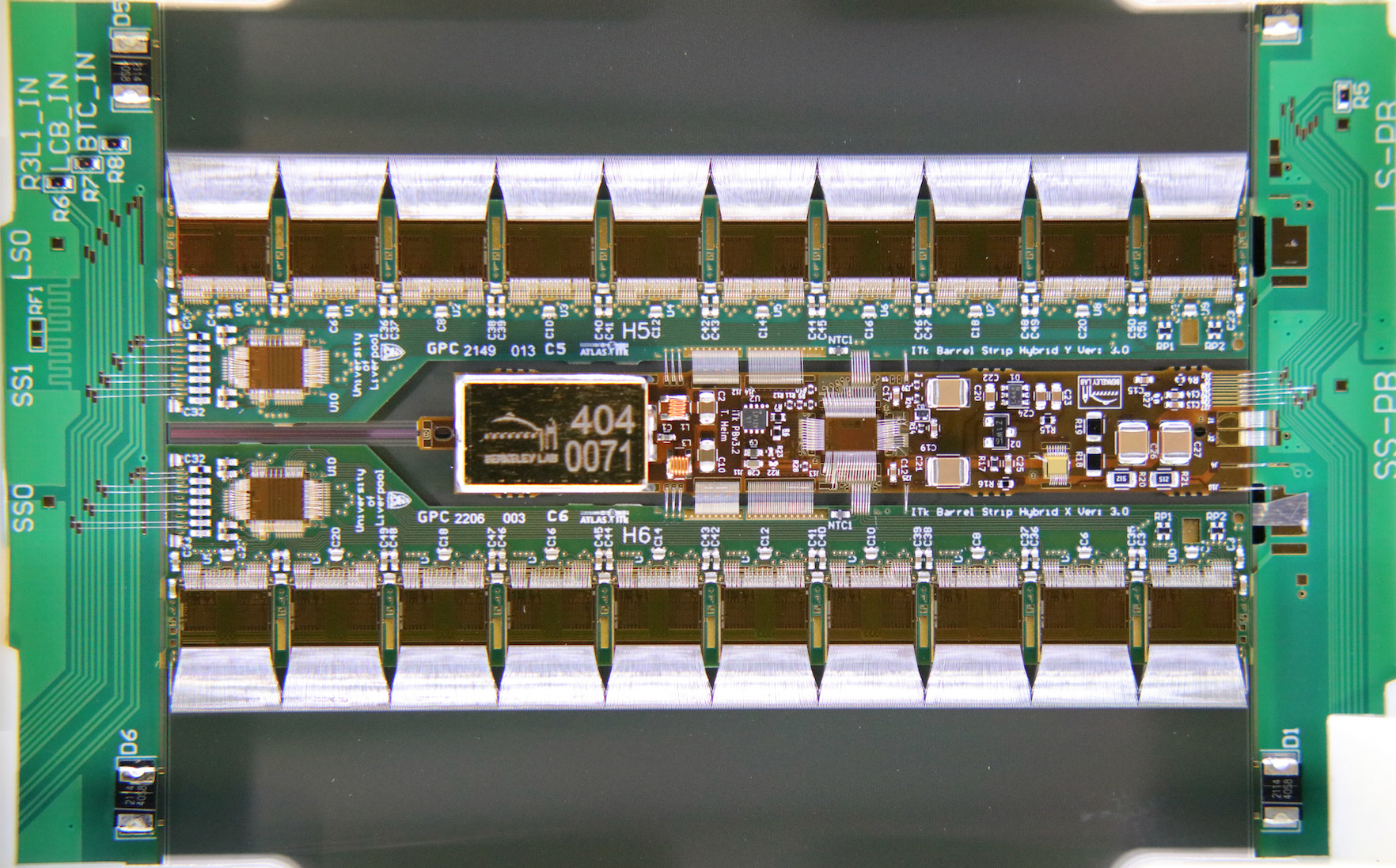 10,000 pixel modules and nearly 18,000 strip modules will be installed in the ITk. Over the next three years, a team of Berkeley Lab physicists, engineers, and technical staff – led by Alessandra Ciocio, a staff scientist in Berkeley Lab’s Physics Division – will fabricate, measure, and test approximately 2,000 of the silicon strip modules as part of its contribution to the ATLAS upgrade. According to Ciocio, “The US will build half of the modules that will be placed on staves, and Berkeley Lab is one of the three U.S. module construction sites. After a long period of prototyping and lab preparation or assembly, and also wire bonding and testing, we are finally ready to produce these modules. All along it was, and still is, a huge team effort. The postdocs and students are playing a key role in the module electrical testing and thermal cycling, metrology measurements, and quality control, all the while gaining knowledge in working closely with the technical staff. Everybody works together to the ultimate goal of producing these modules.” (Photo above: Visual inspection of a production strip module after bonding. 14 of these modules are placed on each side of a stave. Photo credit: Alessandra Ciocio)
The strip modules are placed on “staves” and installed in thin sections on the barrel shells. Berkeley Lab first introduced an integrated stave concept in the late 1990s and early 2000s, and it was originally developed for a different project (as part of the tracker upgrade project planned for the Fermilab Tevatron Collider). The current ATLAS silicon strip tracker was built in the mid-2000s with approximately 4,000 silicon strip modules, and each module was installed independently and sequentially mounted on large carbon fiber barrels.
To address the increased size and complexities of a future tracker, Berkeley Lab senior scientists Carl Haber and Gil Gilchriese continued innovating and proposed a new stave structure in 2008, and this concept was renewed as a viable option to address the needs of the much larger ITk.
Berkeley Lab’s new stave design is a high-performance structure upon which a collection of modules can be pre-mounted and tested. So instead of having to mount 18,000 modules individually, approximately 500 staves can now be slid into pre-mounted fittings and installed onto a barrel shell.
The new stave concept also incorporates an intermediate testing step that accommodates a more highly integrated and multiplexed distribution of the electronic control signals. In this way, a greater bandwidth of signals and controls can be accommodated in the existing space of the ATLAS experiment.
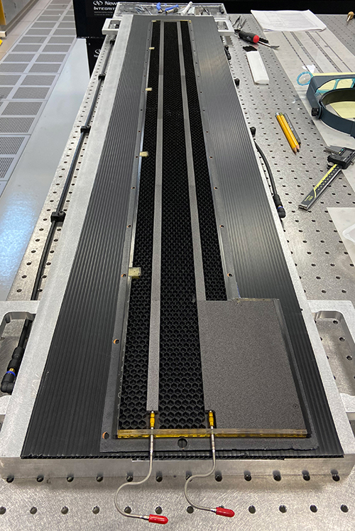 The stave structure was finally realized as a laminated carbon fiber sheet of high modulus (both strong and lightweight) and high thermal conductivity. They are shaped like long planks approximately 120 mm wide, 1,400 mm long, and a few mm thick, and then sandwiched around a core of carbon honeycomb and carbon foam, in contact with titanium cooling pipes. Thin flexible circuits, referred to as “bus tapes,” are cured on the stave’s carbon fiber faces and provide 100% of the electrical services to the modules. The photo at right shows an ATLAS stave core seen during the lamination process, where the inner core of honeycomb carbon has been laminated to the lower carbon facing, and the CO2 cooling lines have been embedded in the honeycomb with a high thermal conductivity carbon foam interface material (Photo credit: Jeffrey Ashenfelder, Yale University). The special carbon foams used within the stave were developed by Allcomp, Inc. (now part of Lockheed), in collaboration with LBNL as part of the DOE Small Business Innovation Research (SBIR) program.
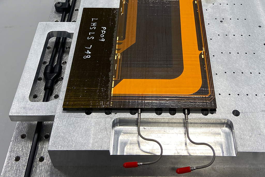
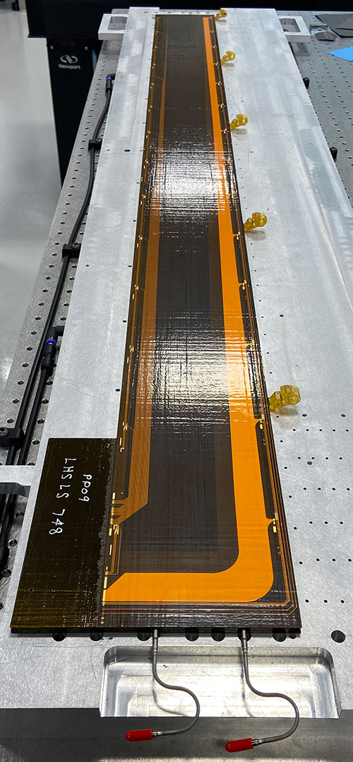 The carbon fiber/bus tape facings are produced in Berkeley Lab’s Composites Workshop and at a similar facility at Oxford University. The final lamination of the stave will occur at Yale University, and the modules will be mounted at Brookhaven National Laboratory. The photo at right is a view of the stave after the full lamination process is completed, and visible now is the topside bus tape, a printed circuit consisting of two layers of etched copper and Kapton polyimide insulation (Photo credit: Jeffrey Ashenfelder, Yale University). The wide track to the right supplies power to the 14 modules that will be mounted on the stave, and the narrow traces on the left supply timing and control signals, and transmit data from the detector.
According to Carl Haber, a senior scientist in Berkeley Lab’s Physics Division, “This project flourished at Berkeley Lab because we have expertise across the thermomechanical technologies of composite materials, the handling and testing of silicon sensors, and front end electronics that goes back four decades.”
Once these staves are completed, Berkeley Lab will be involved in multiple assembly steps to complete the ITk detector over the next 5 years.
###
Berkeley Lab is a multiprogram national laboratory managed by the University of California for the U.S. Department of Energy’s Office of Science (DE-AC02-05CH11231). Berkeley Lab Engineering encompasses a broad range of unique expertise areas, collaborating across a global community of multi-disciplinary researchers to develop instrumentation solutions and technical approaches that address critical scientific problems. Current projects include the design and development of innovative semiconductor detectors, custom integrated circuits, mechanical systems, composite technologies, and complex fabrications, among others. For more information and to learn about job opportunities, visit https://engineering.lbl.gov/. Berkeley Lab’s Physics Division conducts a world-leading program that spans a diversity of research areas including cosmology and dark matter, theoretical and particle physics, quantum information science, machine learning, data science and computing, detector R&D, instrumentation, and microelectronics. Berkeley Lab physicists also lead major experiments including the LZ (LUX-ZEPLIN) Dark Matter Detector, DESI (the Dark Energy Spectroscopic Instrument), and CMB-S4, the next-generation cosmic microwave background experiment. For more information, visit https://www.physics.lbl.gov/.